Published on: September 23, 2026
Alibaba Links a New Custom AI Chip to a 20GW Cloud Infrastructure Roadmap Through 2032
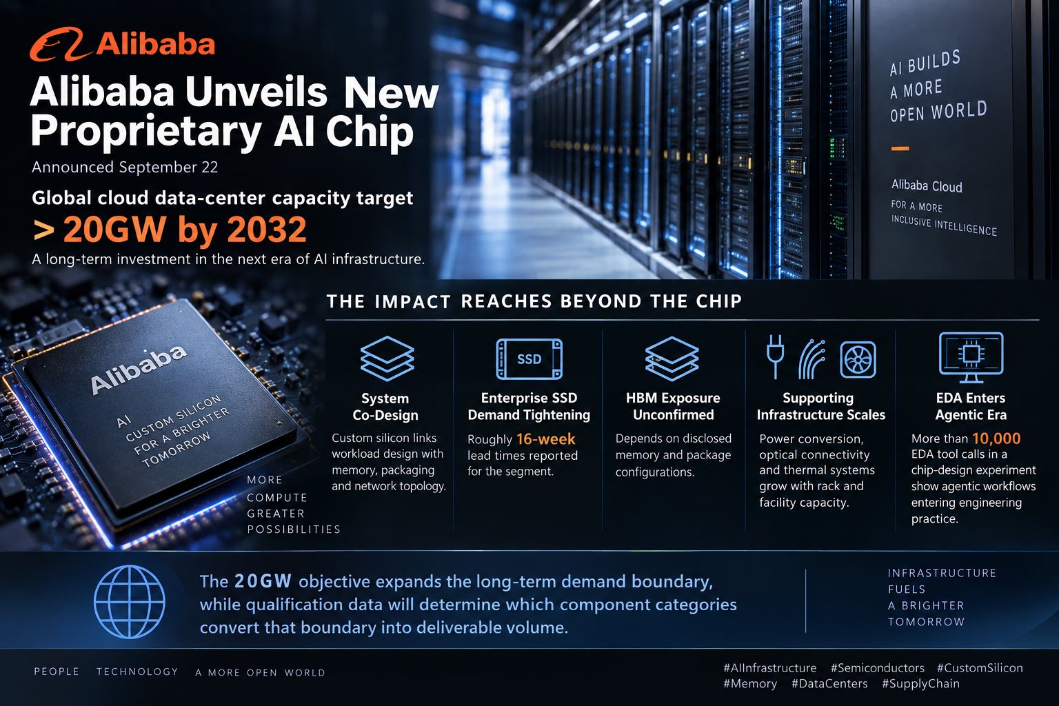
Alibaba announced a new proprietary AI chip on September 22, 2026 and set a target of more than 20GW of global cloud data-center capacity by 2032. The roadmap combines silicon, models, agentic cloud services and physical infrastructure. Process technology, HBM configuration, packaging and production partners remain undisclosed, so strategic demand should be separated from qualified component demand.
A full-stack AI roadmap
Alibaba Cloud used its September 22 Apsara Conference announcement to place a new high-performance proprietary AI chip beside Qwen models, an agentic cloud and mobile-agent services. The release establishes a platform direction but does not disclose the process node, die size, HBM generation, package architecture, interconnect standard or volume-production date. Those omissions matter because a chip announcement does not yet identify a qualified bill of materials.
Custom silicon allows a cloud provider to optimize inference throughput, power, memory capacity, network topology and software together. It can also reduce dependence on a single merchant accelerator architecture. The resulting opportunity extends beyond the compute die to memory, advanced packaging, SerDes, optical links, switches, power management and enterprise storage. Each category still requires configuration-level evidence before a supply conclusion is valid.
More than 20GW by 2032
Alibaba stated that its global cloud data-center capacity is intended to exceed 20GW by 2032. A power target is not a shipment forecast and cannot be converted into a fixed number of accelerators. It nevertheless defines the outer infrastructure envelope. Compute nodes, storage, networking, power delivery, cooling and backup energy must expand together for a deployment of that scale.
At the server level, custom accelerators require host processors, memory, timing, management controllers, network adapters and security components. At the cluster level, switch silicon, DSPs, optical transceivers and connectors rise with fabric density. At the rack and facility levels, higher-voltage distribution increases the importance of power modules, MOSFETs, SiC devices, controllers and sensing. Deployment cadence, rack power and utilization will determine the realized BOM.
Memory architecture remains open
The new chip may use HBM, conventional DDR, LPDDR or a tiered memory architecture. Alibaba has not disclosed the configuration. Training and high-throughput inference would increase the probability that HBM bandwidth and advanced packaging become central constraints. Cost-optimized inference may place greater weight on capacity, bandwidth efficiency and KV-cache tiering across DRAM and enterprise SSDs.
The enterprise-storage signal is already firmer. TrendForce reported on September 21 that North American cloud providers raised fourth-quarter enterprise SSD demand forecasts. Orders could exceed the elevated third-quarter level, with both TLC and QLC contributing. Lead times of about 16 weeks indicate that enterprise NAND allocation has tightened even while consumer NAND faces a different supply-demand balance.
Agentic chip design becomes measurable
Alibaba also described a chip-design experiment in which a model improved for more than 60 hours, made over 10,000 EDA tool calls and produced production-grade bus modules. The result does not automate an entire complex SoC. It does show that specification work, code generation, verification and tool execution can be connected in a measurable engineering loop.
Faster design iteration could increase the number of tape-out candidates, or it could concentrate engineering effort on fewer reusable platforms. The supply impact depends on verification coverage, IP quality, power-performance-area results, EDA licensing and first-silicon success. Design experiments, tape-out, qualification and volume production are separate checkpoints.
Evidence required for supply planning
The next useful disclosures are foundry and process, packaging technology, memory configuration, SerDes rates, system form factor, initial deployment regions and committed production dates. Without those facts, demand can be discussed only by category. Specific lead-time or pricing conclusions require supplier notices, platform BOM evidence or production orders.
Alibaba's roadmap shows cloud providers optimizing models, chips and infrastructure as one system. The 20GW objective expands the long-term demand boundary, while proprietary silicon increases platform-specific qualification. Suppliers with validated components, durable capacity and close system-level integration are positioned for the most defensible share of that expansion.
Deployment timing remains the central uncertainty
The 2032 endpoint covers several semiconductor and server generations. Early facilities may use currently qualified merchant accelerators while later phases introduce a greater share of proprietary silicon. That transition changes the mix of HBM, DDR, storage, optics and power components over time. It also prevents the entire capacity objective from being assigned to one chip design or one manufacturing partner.
Quarterly evidence should include commissioned megawatts, installed rack density, named server platforms, package qualification and confirmed production ramps. Construction announcements without energized capacity do not represent active semiconductor demand. Likewise, a completed chip design does not represent deployment until wafers, packaging, systems and software validation reach the same schedule.